2022 차세대 리소그래피 학술대회

2022 Next Generation Lithography Conference

The Next Decade Visioning for Lithography

Aug. 17 (Wed.) ~ 18 (Thu.), 2022
Suwon Convention Center, Suwon-si, Gyeonggi-do, Korea
Accompanying Event: ASML TechTalk [Aug. 19 (Fri.), 2022]

Plenary Speakers
Plenary Talk 1
AFM Technology for Next Gen Device and Lithography

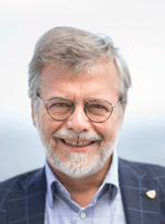
Sang-il Park
Chairman & CEO, Park Systems Corp.

Abstract

Semiconductor technology has been developed and evolved to produce smaller, faster, and less consuming devices for the last several decades. To do so, the device node has been getting smaller and smaller and the lithography technology for photo process has been leading the long journey. The lithography technology is now expanding the boundary of the patterning limitation with a new light source, EUV. In the coming decades, EUV lithography will be a main character of photo process.

In this talk, I’d like to speak about the potential and the future vision of AFM(Atomic Force Microscope) as a nano-metrology and nano-machining solution in the age of sub-10nm device and EUV lithography. AFM has proven its advantages in non-destructively measuring the dimensions(height and width) of nanostructures in semiconductor industry, without requiring a special environment such as vacuum or pre-treatment of samples. And AFM has expanded its applications to measuring the electrical and physical characteristics of nanoscale areas of the chip or defects of interest for defect analysis using the tiny probe tip. Moreover, it will enable chemical identification of nanoscale areas or defects in semiconductor and other industrial applications combined with a photo-induced force microscope(PiFM) technology. AFM also has nano-machining capabilities and plays a key role by providing a defect repair solution to remove the particles and pattern defects on EUV/DUV masks in lithography area.

Biography

Dr. Sang-il Park is the founder, chairman and CEO of Park Systems Corporation. Dr. Park led the adoption of the Atomic Force Microscope (AFM) as a mainstream scientific instrument through the development of the first commercially viable AFM. Through Dr. Park’s first commercialization, sharing of the key technology with the competition, and his ensuing innovations, the AFM has become one of the most utilized and crucial nanoscience and nanotechnology instruments driving great progress in all fields of science, engineering, and semiconductor manufacturing.

Dr. Park is a popular speaker at conferences and has given hundreds of seminars at leading academic institutions and industry trade events world-wide showcasing the AFM and nanotechnology innovations. As a leading spokesperson to media about nanoscience and the economy, Dr. Park was a participant in the Presidential Advisory Council for Science and Technology and on the Future Preparation Committee in Korea.

Dr. Park obtained a B.S. in Physics from Seoul National University in 1981 and a Ph.D. from Stanford University in 1987. He has also a Mini MBA degree from the Stanford-AEA Executive Institute. His research interests are nanotechnology, nanometrology, and scanning probe microscopy and its applications. He authored and co-authored numerous research papers, textbooks, and over twenty U.S. patents in the field of Atomic Force Microscope.
Plenary Talk 2
Social Value of NGL

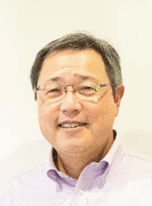
Jae Hyun Kim
Fellow, Future Tech R&D Center, SK hynix

Abstract

Lithography technology has been innovated and developed last 50 years to make smaller node patterns and enable Moor’s law scaling down to 3nm. Whenever resolution limitation encountered, the whole semiconductor industry introduced shorter wavelength light and novel technologies to overcome any hurdles in semiconductor shrinking trend. Due to these cumulative actions to make new NGL, lots of development in electronic devices have changed in our routine life comparing with 50 years in communications, transportation, way of working, manufacturing, commerce and even hobbies.

Nowadays, many people like to evaluate not only economic value of new companies or technologies but also social value of them to estimate the sustainability their existence. In the past, output performance based on input resource would be major criteria to check the success of any tries. Every company and technology have been evaluated on the basis of this economic value and has focused to improve the efficiency. But this efficiency-based barometer cannot always guarantee the success of companies and technologies. This is the reason why people started to evaluate social values as well as economic value.

In this talk, I will try to think about what the social value of NGL could be. Lithography society has developed new technologies to make smaller node size device and contributed lots of economic value by reducing the cost for manufacturing a bit. Bit- growth and bit-cross have been major driving force to require NGL in semiconductor industry. All this justification can explain the economic value of NGL. Not only output and outcome but also impact from the given input in lithography technology is worthwhile to consider social value of NGL and understand the sustainability of our activities. In addition, I will add what would be current necessary our tasks to make more big social value of NGL for the time being

Biography

“Jae Hyun Kim”, Ph.D. has been material development position at SK hynix since September 2021 with major responsibility of EUV patterning material development. With the current position, he has focused on high performance EUV materials development pursuing competitive EUV process and on novel platform establishment for the efficient material development environment.

Prior to joining SK hynix, Dr. Kim used to be a group leader at Foundry division in Samsung Electronics by July 2019. During his 19 years at Samsung Electronics, he has been spent 6 years leading foundry material technology group responsible for all kinds of semiconductor manufacturing materials, 1.3 years dispatching as an expatriate at Samsung Austin, 2 years developing new lithographic and packaging material development at R&D center, and 10 years leading novel patterning material development at Memory division from September 2000.

Dr. Kim received a EMBA degree in Economics and Management department at Tsinghua University, Beijing, China and at INSEAD, Fontainbleau, France in January 2021 and got Ph.D. degree in Chemical Engineering department at Seoul National University, Korea in August 2000. During his EMBA, Dr. Kim researched the impact of the US-China Trade Conflicts on the Global Semiconductor Industry and during his Ph.D. study, Dr. Kim investigated the thickness effect on physical properties of thin polymer films down to 20nm.
Plenary Talk 3
The (R)Evolution of Lithography Optics from UV to EUV

Winfried Kaiser
ZEISS Fellow (retired), Carl Zeiss SMT GmbH

Abstract

In recent years the promise of EUV Lithography to combine highest resolution with high productivity became reality and so enables HVM of the most advanced chips. EUVL marks the latest technology leap in the more than five decades of progress in lithography. Since the resolution of the lithography optics is tightly correlated with the critical dimensions of an IC the progress in optics is seen as a key enabler of Moore’s Law. To achieve the higher and higher optical resolution it was necessary several times to switch to shorter exposure wavelengths from initially blue light (g-line, 436nm) to latest EUV (13.5nm) in parallel to the realization of higher Numerical Apertures (NA) of the projection optics.

Now more than 100 highly complex and precise ASML NXE scanners with their ZEISS EUV optics are installed in the field and are exposing millions of wafers in the fabs. To enable a resolution of 13nm this generation of EUV optics has a NA of 0.33. In this presentation we will explain the general set up of the EUV optical system including its specific challenges and we will give insights into the actual production status at ZEISS and the ongoing improvements.

To continue Moore’s Law and to enable even more advanced chips with smaller critical dimensions in the future ASML and ZEISS are developing a next generation EUV system named “High NA EUV” with an even higher resolution based on a NA of 0.55 – an increase of 67%, the biggest boost ever made in the history of lithography! To produce these huge optical systems a completely new manufacturing infrastructure is needed at ZEISS. We will explain the layout of these optics and report on the status of the installations and of the project.

Biography

Winfried Kaiser studied Physics and Technical Optics at the Universities of Tübingen and Stuttgart and received his Diploma in 1982. He joined ZEISS in 1982 as a scientist and has held several management positions since. In 1995 he initiated the cooperation on EUV in Europe. Until his retirement in 2020 he was Senior Vice President “Product Strategy” of Carl Zeiss SMT GmbH.

Winfried Kaiser is a recipient of the 2006 European SEMI Award and has been promoted to “Carl Zeiss Fellow” in 2007. In 2008, he was named “Fellow of the SPIE Society” and introduced into the Chip Making Industry Hall of Fame. He received the SEMI “Bob Graham” SME Excellence Award in 2014 and the SPIE Frits Zernike Award in 2020.
Plenary Talk 4
EUV HVM Status and the Roadmap Update

Kenji Morisaki
Director & Head of Field Marketing (Japan), ASML

Abstract

This presentation will provide a current EUVL HVM implementation progress including the field performance data from multiple NXE:3400C and NXE:3600D systems proving the capability to support 5nm and the beyond device node. Then updating ASML’s EUV roadmap both for 0.33NA and 0.55NA (High-NA) EUV systems. And finally, it will provide update current High-NA EUV system development status.

Experience

  • 2004 – Present : ASML
  • 1999 – 2004 : KLA-Tencor Japan (Analyst, Regional product manager)
  • 1987 – 1999 : Fujitsu (Litho Process engineer)
Biography

After graduation of Yokohama National University, he joined Fujitsu as a litho process engineer where he experienced various roles from process development to technology transfer for mass production including simulation, tool/material selection, mask design etc. and also joint venture project as an assignee to oversees partner company.

Then he joined KLA-Tencor as an analyst at yield management consulting group where he engaged various project globally, also he worked as regional product manager for litho solution products covering Asia-Pacific region.